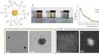
Nanotubes are tiny, cylindrical structures made of carbon atoms. They are only a few nanometers in diameter, which is about 100,000 times smaller than a human hair. Because of their small size, nanotubes are difficult to see with traditional optical microscopes. However, they can be made visible using an electron beam.
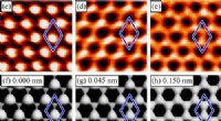
An electron beam is a stream of high-energy electrons. When an electron beam strikes an object, the electrons interact with the atoms in the object and scatter. The scattering pattern can be used to create an image of the object.
In the case of nanotubes, the electron beam scatters off of the carbon atoms in the nanotube walls. The scattered electrons are then detected by a sensor, which creates an image of the nanotube.
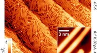
Electron beam microscopy is a powerful tool for imaging nanotubes. It allows scientists to see the detailed structure of nanotubes and to study their properties.
Here is a more detailed explanation of the process of electron beam microscopy:
1. A beam of high-energy electrons is generated by an electron gun.
2. The electron beam is focused onto the sample.
3. The electrons interact with the atoms in the sample and scatter.
4. The scattered electrons are detected by a sensor.
5. The sensor creates an image of the sample based on the scattering pattern.
The resolution of an electron microscope is determined by the wavelength of the electrons. The shorter the wavelength, the higher the resolution. However, shorter wavelengths also mean that the electrons have more energy and can damage the sample.
Therefore, the choice of electron wavelength is a trade-off between resolution and sample damage.
Electron beam microscopy is a versatile technique that can be used to image a wide variety of materials. It is particularly well-suited for imaging small, delicate structures like nanotubes.