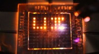
Large-area growth of atomically thin, layered semiconductors. Credit: Nature 520, 631–632 (30 April 2015) doi:10.1038/520631a
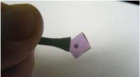
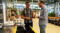
(Phys.org)—A team of researchers at Cornell University has developed a technique that allows for growing 3 atom thick semiconducting films on wafers, up to 10 centimeters across. In their paper published in the journal Nature, the team describes their technique and the ways it might be used to create ultra-tiny circuits. Tobin Marks and Mark Hersam of Northwestern University offer a News & Views perspective piece on the work done by the team in the same journal issue.
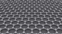
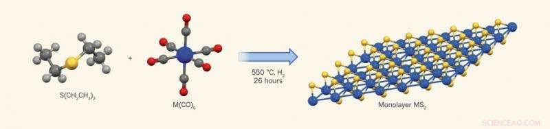
As the search continues for ways to allow for creating smaller and smaller circuits, researchers have turned to what are known as 2D materials, those that are just an atom thick—which at this point, appears to be a physical limit. Testing of such materials has proven fruitful and scientists are convinced that someday soon, they will be used in all manner of electronic gizmos. The thing holding them up right now is a means of mass producing them in sizes that are large enough to be useful while remaining homogenous across their entire surface (having spatial uniformity). In this new effort, the researchers have found success by modifying a process known as metal organic chemical vapor deposition (MOCVD) to create two types of transition-metal dichalcogenides (TMDs)—tungsten disulfide and molybdenum disulfide. One layer of the material is three atoms thick and it was created without having to resort to using sticky-tape, and unlike graphene, it is a semiconductor.
The team created their films by growing them on insulating SiO2 substrates using a metal–organic chemical vapor deposition technique. In creating 200 of the films, they found just two that failed to conduct properly—a 99 percent success rate. In testing, the films were found to be not just uniform, but comparable in performance to films created using the sticky-tape method. They note that the key to success was sourcing each of the ingredients from gasses, where every molecule had only one atom of the transition metal. Altering the gas pressure, they noted allowed for controlling the degree of concentration of the ingredients and thus the film's growth.
The researchers believe the large size of the films should allow for the creation of devices that use them, though more work will have to be done to ensure the technique will allow for growing films on other surfaces, particularly those that are flexible.
© 2015 Phys.org