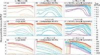
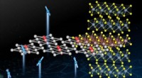
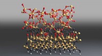
Multilayer 2-D materials are composed of multiple layers of atoms stacked together. The interactions between these layers can significantly influence the material's electrical properties. For example, the interlayer coupling in graphene can lead to the formation of quantum well states and Dirac cones, which give rise to unique electronic transport phenomena.
One important aspect of current flow in multilayer 2-D materials is the role of interlayer transport. In these materials, electric current can flow not only within each individual layer but also between different layers. The interlayer transport can be mediated by various mechanisms, such as direct tunneling, phonon-assisted tunneling, and defect-assisted transport. Understanding and controlling these interlayer transport mechanisms is crucial for designing high-performance electronic devices based on multilayer 2-D materials.
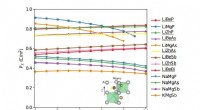
Another key factor that affects the current flow in multilayer 2-D materials is the presence of defects and impurities. Defects can act as scattering centers for electrons and hinder their transport. Therefore, reducing defects and impurities is crucial for improving the material's electrical conductivity. Techniques such as chemical vapor deposition (CVD) and molecular beam epitaxy (MBE) are commonly used to grow high-quality multilayer 2-D materials with minimal defects.
Scientists are also investigating the effects of strain and external fields on the current flow in multilayer 2-D materials. Strain can modify the material's electronic band structure and interlayer interactions, leading to changes in the electrical conductivity and other transport properties. External fields, such as magnetic fields and electric fields, can also influence the current flow and give rise to interesting magnetotransport and electrotransport phenomena.
In summary, scientists are actively investigating how electric current flows in multilayer 2-D materials. By understanding the role of interlayer transport, defects, strain, and external fields, researchers aim to optimize the electrical properties of these materials and unlock their full potential for next-generation electronic device applications.