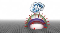
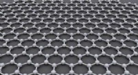
The introduction of flexible electronics was a paradigm change on established technologies. Now, researchers at the Barcelona Institute of Science and Technology (BIST), present a versatile, low-cost and customizable method for patterning graphene oxide onto multiple substrates. This patented technique, published in the latest issue of ACS Nano, might also be applicable to other electronic materials.
Some methods for patterning electronic devices involve long fabrication periods, high cost, great expertise and clean room facilities. Moreover, these methods are not versatile or effective for designing simple devices such as transistors or capacitors and biosensors that require effective linking of specific bioreceptors. The patterning method by ICN2 allows the transfer of graphene oxide onto almost any substrate in an easy, cost-effective and customizable way.
The patented method consists of three steps:
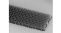
This green, low-cost and versatile approach will enable in situ transfer of multiple electronic devices such as field effect transistors (FET), LEDs, electrodes, solar cells, biosensors or supercapacitors. It requires neither a clean room nor organic solvents. The wax-printed membranes have 50μm resolution, long-term stability and infinite shaping capability over a variety of substrates, including textile, paper, adhesive film or PET. Additionally, the technology can be implemented in a roll-to-roll hardware, speeding up the printing. It is also is promising for implementation in under-developed countries.
For further information: Download the patented technology flyer.