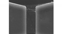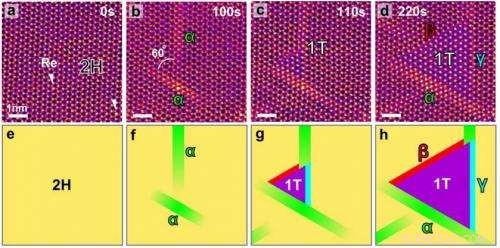
Evolution of 2H → 1T phase transformation in SL-MoS2 at T=600°C. Credit: Nature Nanotechnology (2014) doi:10.1038/nnano.2014.64
(Phys.org) —A team of researchers with members from Japan, Taiwan and Switzerland has discovered that it is possible to watch a phase transition occur in a 2D semiconducting material using a scanning transmission electron microscope (STEM). In their paper published in the journal Nature Nanotechnolgy describing their research and results, the team outlines how they used the microscope to watch as a sample of the direct bandgap semiconductor molybdenum sulphide underwent a phase shift.
An ability to phase shift between metallic capabilities and a semiconductor is an important feature of a material—one that scientists would like to better understand. Up till now however, researchers had to infer some of what occurs when a material undergoes a phase shift, because they couldn't actually see it as it was happening. In this new effort, the researchers show that it is possible to directly watch a phase shift by doing so with a sample of molybdenum sulphide. In so doing, they have discovered that atom-by-atom movements are part of the shift, rather than complete shifts by a collective. The researchers suggest their observations hint at the prospect of creating layered 2D semiconductors "in-layer" rather than as a series of steps where one material is layered over another. That would allow for creating structures with atomic scale precision.
Molybdenum sulphide is polymorphic—it can function as either a metal or a semiconductor, depending on how much heat is present. Even better the two phases can be made to interconvert using intralayer atomic plane gliding, (a transversal displacement of one of the materials across the other) though it had never been seen actually doing so. As part of their research, the team performed in situ plane gliding while watching using the STEM, giving them an unprecedented view of what actually occurs as such phase shifting happens. The phase shift with the molybdenum sulphide sample occurred due to the heat exerted by the STEM itself. They suggest such a technique could also be used to induce phase shifting in other 2D materials.
The researchers also report that they have already used what they have learned to create several prototype nanodevices—one of which performs the functions of a Schottky diode.
© 2014 Phys.org