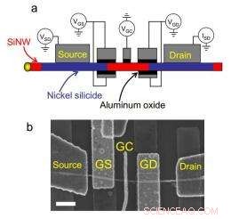
a) Schematic of a multi-gate device made from a single, undoped SiNW. Two wrap-gates, labeled as GS and GD, are designed to control the Schottky barriers at the silicidesilicon junctions formed by the source and drain contacts. The finger gate in the middle, labeled as GC, is meant to control carrier population in the silicon channel. b) SEM micrograph of the device. Scale bar: 400nm. Image: arXiv:1208.1465v1
(Phys.org) -- A team of French physicists working out of Universite Joseph Fourier, France, has found a way to create logic gates, transistors and diodes from silicon nanowires without having to resort to dopants (inserting another material into the original to change its electrical or optical properties). Their process, which they explain in the paper they’ve written and uploaded to the preprint server arXiv, involves applying a very thin layer of silicates at the juncture of metal and nanowires.
For quite some time researchers have been looking for a way to create silicon nanowires that could be used in actual devices because they would be so much easier to make than having to use conventional photolithography, i.e. etching. They’ve been stymied however by one little problem. When trying to connect the tiny nanowires to the rest of the electronics, using metal contacts, they bump up against what is known as the Schottky barrier. This is where the electrons in the metal push back against those in the semiconductor allowing current to flow in only one direction; a feature that might be useful in some applications, but not when trying to build transistors or logic gates because of the need for rectification.
To get around this problem, researchers have tended to use various doping techniques which have thus far proved unreliable because the dopants require precise placement at the nanoscale level, a difficult feat to achieve and which in most cases has led to variable levels of performance.
The French team took another approach, instead of doping the materials, they instead applied a thin film of metal silicate to the nanowire at the point where it meets the metal contact, and that was all it took to prevent a Schottky barrier from occurring. With that problem solved, they then built a bipolar transistor and two types of diodes and eventually a NAND gate.
Their approach will have to be further tested and analyzed by other research teams, of course, but their results are clearly promising. If everything works out as envisioned, we may very soon see nanowires being used in devices such as biosensors and optoelectronics.
© 2012 Phys.org