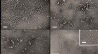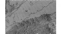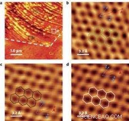
The first scanning tunneling microscopy (STM) images of graphene synthesized on copper foil. (b-d) show atomic-resolution images at various locations of the large graphene domain shown in (a).
Users from Purdue University, working collaboratively with staff in the CNM Electronic & Magnetic Materials & Devices Group, studied CVD-grown graphene on polycrystalline copper foil for the first time at the atomic-scale. The ultrahigh vacuum scanning tunneling microscopy (UHV-STM) findings performed at CNM will help to guide the optimization of synthesis towards defect-free graphene.
The focus of this study was to investigate the quality of the films and relative orientations of different graphene domains using the UHV-STM facility at CNM. The recent paper also addresses the resulting implications for domain boundary effects on transport properties.
The work follows previous studies done at CNM that investigated graphene on single-crystal Cu(111). Similar to the single-crystal work, it was shown that domain boundaries dramatically affect the carrier mobility of the graphene sheets. The ability to synthesize high-quality graphene for large-scale integration is one of the key challenges for this material system. Fundamental STM experiments performed at the atomic-scale have enabled the study of defects in the as-grown films.
Researchers from the University of Houston, Texas State University, Carl Zeiss SMT, and the Center for Functional Nanomaterials also participated in the study, which is featured as the cover image of Nature Materials.