Here's a breakdown of its capabilities:
Visualization:
* Atomic resolution imaging: SPMs can produce images with resolutions down to the angstrom level (10^-10 meters), allowing scientists to see individual atoms and molecules.
* Surface topography: SPMs can map the three-dimensional structure of surfaces, revealing details like bumps, valleys, and even individual molecules.
* Material properties: SPMs can detect and map various material properties like electrical conductivity, magnetic properties, and mechanical properties at the nanoscale.
Manipulation:
* Atomic manipulation: Certain types of SPMs (like the atomic force microscope, AFM) can be used to move individual atoms and molecules, allowing for the construction of nanoscale structures.
* Nanofabrication: SPMs can be used to create nanoscale patterns and structures on surfaces, paving the way for advanced nanotechnology applications.
Types of Nanoscopes:
* Scanning Tunneling Microscope (STM): Uses a sharp tip to scan a conducting surface, measuring the tunneling current to create images.
* Atomic Force Microscope (AFM): Uses a sharp tip to scan a surface, measuring the forces between the tip and the surface to create images.
* Near-field Scanning Optical Microscope (NSOM): Combines the principles of optical microscopy with SPM techniques to overcome the diffraction limit of light microscopy.
Applications of Nanoscopes:
* Materials science: Characterizing and understanding materials at the atomic level.
* Nanotechnology: Developing new materials and devices at the nanoscale.
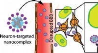
* Biotechnology: Imaging and manipulating biological molecules and structures.
* Electronics: Investigating and creating novel electronic devices.
In summary, nanoscopes are powerful tools that allow us to see and manipulate matter at the most fundamental level, driving innovation in various scientific and technological fields.