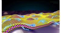
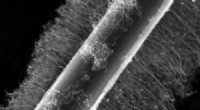
High Surface-to-Volume Ratio: Nanowires have a very high surface-to-volume ratio, which means that a large number of atoms are located at the surface of the nanowire. This is beneficial for photodetection because the absorption of light occurs at the surface of the semiconductor material. The high surface-to-volume ratio of nanowires allows for efficient light absorption and charge carrier generation.
Enhanced Light Absorption: The small size and high surface-to-volume ratio of nanowires enable enhanced light absorption. Nanowires can effectively capture and guide light within their structures, leading to increased interaction between the light and the semiconductor material. This significantly improves the photodetector's light sensitivity and responsivity.
Direct Bandgap: Many nanowire materials, such as gallium arsenide (GaAs) and indium phosphide (InP), have a direct bandgap. This means that the energy levels of electrons and holes in these materials are aligned in a way that allows for efficient absorption and emission of light. This direct bandgap property contributes to the high photodetection efficiency of nanowires.
Tunable Properties: The properties of nanowires, such as their bandgap, carrier concentration, and surface chemistry, can be precisely controlled during synthesis and fabrication. This tunability allows for the customization of nanowire photodetectors to meet specific requirements and applications. By controlling the nanowire dimensions, doping levels, and material composition, the spectral response, sensitivity, and other characteristics of the photodetector can be optimized.
Fast Response Time: Nanowires have a fast response time due to their small size and short carrier diffusion lengths. The small dimensions of nanowires enable rapid separation and collection of photogenerated charge carriers, leading to fast detection of light signals. This fast response time makes nanowire photodetectors suitable for high-speed applications, such as optical communication and imaging.
Versatility and Integration: Nanowires can be integrated with various materials and device architectures, providing versatility in photodetector design. They can be combined with other semiconductors, metals, dielectrics, and optical components to create sophisticated photodetector structures. This flexibility allows for the development of integrated photodetector arrays, multi-spectral detectors, and more complex optoelectronic systems.
These properties make nanowires attractive materials for photodetectors in various applications, including optical communication, imaging, spectroscopy, environmental sensing, and medical diagnostics.