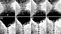
Nanobridges are tiny structures that consist of a narrow strip of material that connects two larger pieces of material. They are often used in electronic devices to control the flow of current. However, traditional methods for creating nanobridges are complex and time-consuming, making them impractical for mass production.
The new technique developed at Berkeley uses a process called "self-aligned nanowire lithography" to create the nanobridges. This process begins with the deposition of a thin layer of material, such as silicon or metal, onto a substrate. The material is then patterned using a lithographic process to create a series of narrow lines. These lines are then etched using a reactive ion etch (RIE) process to form the nanobridges.
The advantage of this technique is that it allows for the precise placement of individual nanobridges with a high degree of accuracy. This is important for the development of nanoscale devices, as the precise positioning of components is essential for proper operation.
The researchers demonstrated the technique by creating a series of nanobridges with different widths and lengths. They found that the nanobridges could be accurately positioned with a tolerance of less than 10 nanometers. This level of accuracy is sufficient for the development of many nanoscale devices.
The researchers believe that the self-aligned nanowire lithography could potentially reduce the cost and complexity of manufacturing nanoscale devices. This could open up new possibilities for the development of a wide range of nanoscale electronic devices, including transistors, sensors, and NEMS.
The research was published in the journal Applied Physics Letters.