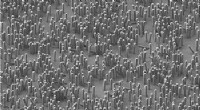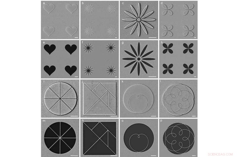
(a-d) and (i-l) Multiscale metal micro-nano positive-type structures with sharp features or extremely small gaps; (e-f) and (m-p) the corresponding inverse metallic structures after lift-off. All scalebars: 1 µm. Credit: Science China Press
Photoresist-based patterning strategies have been standardized for decades since the invention of photolithography. However, there are still major challenges in the processing of certain functional structures. For example, the standard resist-based high resolution patterning process usually requires point-by-point exposure of the target resist structures, leading to extremely low throughput and an unavoidable proximity effect when defining multiscale patterns; high-energy beam irradiation can easily cause damage to the materials; and the negative-tone-resist-based lift-off process is challenging.
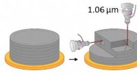
Recently, the journal National Science Review published the results of Professor Duan Huigao's research group from Hunan University. The team proposed and demonstrated a new resist patterning strategy, called "resist nano-kirigami." The outline of the target structure is exposed on the resist, and the excess resist film is selectively mechanically stripped. Compared with traditional electron beam lithography, this scheme has the following core advantages:
The strategy provides a new patterning solution that expands the family of lithography techniques and will play a significant role in fabricating multiscale functional structures. + Explore further