Here's how it works:
1. Electron Beam: A focused beam of electrons is directed at the surface of the sample.
2. Interaction: The electrons interact with the sample's atoms, causing some electrons to be scattered or emitted.
3. Signal Detection: Detectors collect these scattered or emitted electrons, providing information about the sample's surface.
4. Image Formation: The signals are processed to create an image that reveals the sample's surface topography, composition, and other properties.
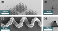
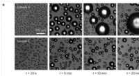
SEMs are powerful tools for visualizing the surface details of materials at a very high resolution, often in the nanometer range. They are widely used in various fields like materials science, biology, and nanotechnology.