Quantum Confinement Effects:
2-D materials, especially when thinned down to a single atomic layer, exhibit pronounced quantum confinement effects. The confinement of electrons and holes in the vertical direction leads to discrete electronic states and modifies their energy dispersion, bandgap, and other electronic properties. By varying the thickness of the 2-D material, these quantum confinement effects can be systematically studied, allowing researchers to understand how the electronic properties evolve as dimensionality changes.
Tuning Bandgap and Electronic Structure:
The thickness of 2-D materials can significantly influence their bandgap and electronic structure. For instance, in transition metal dichalcogenides (TMDCs), the bandgap can change from indirect to direct as the number of layers decreases, resulting in a transition from a semiconductor to a quasi-metallic behavior. By controlling the thickness, it becomes possible to tailor the electronic properties of 2-D materials for specific applications, such as optoelectronics, nanoelectronics, and energy harvesting.
Probing Interlayer Interactions:
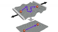
In van der Waals heterostructures, where two or more 2-D materials are stacked together, the interlayer interactions play a crucial role in determining the overall electronic properties. Varying the thickness of one of the layers alters the interlayer distance and strength of these interactions, allowing researchers to investigate how the coupling between individual layers affects the electronic structure, charge transport, and other properties of the heterostructure.
Emergent Phenomena:
2-D materials often exhibit novel and unexpected phenomena that emerge only in the two-dimensional limit. For example, certain 2-D materials can host unconventional superconductivity, topological insulators, and strongly correlated electron states. Measuring thickness-dependent electronic properties helps elucidate these emergent phenomena and explore their underlying physics, which could lead to groundbreaking applications in quantum technologies, spintronics, and nanoelectronics.
Scalability and Device Integration:
Studying 2-D materials in thin layers or as monolayers is essential for their practical implementation and integration into devices. Monolayer or few-layer 2-D materials are often required for achieving optimal performance and minimizing defects or disorder. By understanding thickness-dependent electronic properties, researchers can optimize device architectures and fabrication processes to harness the full potential of 2-D materials in various applications, such as transistors, photodetectors, and energy storage devices.
In summary, measuring thickness-dependent electronic properties in 2-D materials offers a systematic approach to exploring their unique quantum confinement effects, tunable bandgaps, interlayer interactions, and emergent phenomena. This understanding is critical for designing and optimizing 2-D material-based devices with tailored electronic properties for cutting-edge applications in nanoelectronics, optoelectronics, quantum technologies, and beyond.