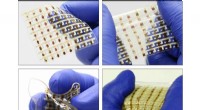
Gallium nitride (GaN) is a promising semiconductor material for high-power and high-frequency electronic devices, such as transistors. However, GaN transistors have traditionally suffered from poor reliability due to the formation of defects at the interface between the GaN layer and the substrate, which can lead to device failure.
Recently, researchers have discovered that depositing a thin layer of diamond on the GaN layer can significantly improve the reliability of GaN transistors. The diamond layer acts as a protective barrier that prevents the formation of defects at the interface, leading to longer device lifetimes.
This breakthrough has the potential to revolutionize transistor technology and enable the development of more powerful and efficient electronic devices. GaN transistors with diamond layers could be used in a wide range of applications, including power electronics, radio frequency communications, and high-brightness light-emitting diodes (LEDs).
Here are some of the key benefits of using diamonds as a protective layer for GaN transistors:
* Improved reliability: The diamond layer prevents the formation of defects at the GaN/substrate interface, leading to longer device lifetimes.
* Higher power density: GaN transistors with diamond layers can operate at higher power densities than conventional GaN transistors, enabling the development of more compact and efficient electronic devices.
* Higher efficiency: Diamond layers can improve the efficiency of GaN transistors by reducing the leakage current.
* Broadband operation: GaN transistors with diamond layers can operate over a wider frequency range than conventional GaN transistors, making them suitable for a variety of applications.
The combination of GaN and diamond is a promising new material system for high-power and high-frequency electronic devices. With the development of reliable GaN transistors with diamond layers, we can expect to see a new generation of electronic devices that are more powerful, efficient, and compact.