Here's why:
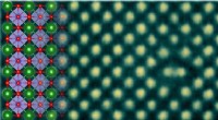
* STM works by quantum tunneling: It uses a sharp, conductive tip that is brought very close to the surface of the metal. The tip and the metal surface are held at a specific voltage difference, and electrons can "tunnel" across the gap between them.
* Detecting the tunneling current: By measuring the current flow, the STM can map the surface at the atomic level. This is because the tunneling current is very sensitive to the distance between the tip and the surface.
* Revealing surface details: By scanning the tip across the surface, the STM can create a detailed image of the arrangement of atoms.
Other techniques that can be used to study the surface of materials:
* Atomic Force Microscopy (AFM): This technique uses a sharp tip to "feel" the surface, providing information about its topography and mechanical properties.
* X-ray Photoelectron Spectroscopy (XPS): This technique uses X-rays to probe the elemental composition and chemical state of the surface.
While these techniques can provide information about the surface, only the STM can directly image the arrangement of individual atoms.