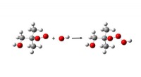
The research team, led by scientists from the University of California, Berkeley, employed a technique known as "nanoconfinement" to restrict the motion of charge carriers within a material. By fabricating nanostructures that confine electrons and ions to specific regions, they were able to manipulate the material's properties at the nanoscale.
One of the key findings of the study was the ability to enhance the material's electrical conductivity by creating one-dimensional channels that guide the flow of electrons. By controlling the size and arrangement of these channels, the scientists could precisely tune the material's electrical properties, making it more efficient for conducting electricity.
In addition to improving electrical conductivity, nanoconfinement also allowed the researchers to modify the material's optical properties. By controlling the confinement of electrons and ions, they could alter the material's refractive index, which determines how light interacts with the material. This enabled the creation of materials with tailored optical properties for applications in optoelectronics, such as lasers and optical fibers.
Furthermore, the study revealed that nanoconfinement can influence the magnetic properties of materials. By confining electrons and ions within specific regions, the researchers could induce magnetic ordering, even in materials that are typically non-magnetic. This finding holds promise for the development of novel magnetic materials for use in data storage, spintronics, and magnetic sensors.
Overall, the ability to precisely control the transport of electrons and ions within a material using nanoconfinement opens up exciting avenues for materials design and engineering. By harnessing this technique, scientists can create advanced materials with tailored properties for a wide range of applications, advancing fields such as electronics, energy storage, catalysis, and optics.