1. Semiconductors: In semiconductor materials, defects can create localized energy states within the bandgap, altering the material's electrical properties. This is the foundation of semiconductor device technology, where specific defects or dopants are intentionally introduced to control the conductivity, carrier concentration, and electronic properties of semiconductors. By engineering defects, we can create transistors, diodes, solar cells, and other essential electronic components.
2. Luminescence and Phosphors: Defects can act as luminescent centers in materials, allowing them to emit light of specific colors when exposed to energy sources such as ultraviolet light or electrical currents. This property is exploited in various applications, including phosphors for fluorescent and LED lighting, color filters, and medical imaging. By manipulating defects, we can control the emission wavelength, intensity, and persistence of luminescence.
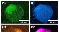
3. Magnetic Materials: Defects can introduce magnetic moments in non-magnetic materials or modify the magnetic properties of existing magnetic materials. This phenomenon is known as defect-induced magnetism and finds applications in magnetic recording media, spintronics, and the development of novel magnetic materials. By controlling defects, we can tune magnetic properties such as coercivity, remanence, and susceptibility.
4. Photocatalysis: Defects can enhance the photocatalytic activity of materials, which involves the conversion of light energy into chemical energy. By introducing defects, we can create active sites on the material's surface that facilitate the absorption of light and the subsequent chemical reactions. This is important for applications such as water splitting, pollutant degradation, and solar fuel production.
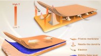
5. Battery Materials: Defects can play a crucial role in the performance of battery materials, particularly in lithium-ion batteries. Certain defects can improve the intercalation/deintercalation kinetics of lithium ions, enhance the cyclability and lifespan of batteries, and reduce the voltage hysteresis. By controlling defects, we can optimize battery efficiency, capacity, and longevity.
6. Sensors and Gas Detection: Defects can be utilized to create highly sensitive sensors for detecting specific gases, vapors, or chemical compounds. The defects act as active sites that selectively interact with the target molecules, leading to changes in electrical properties, optical properties, or other measurable parameters. This enables the development of gas sensors, chemical sensors, and biosensors for various applications.
These are just a few examples of how defects can transform inert materials into useful, active ones. By understanding and controlling defects, materials scientists and engineers can unlock new functionalities and properties, paving the way for innovative technologies and applications.